بلاكويل (عمارة دقيقة)
 | |
| سيُطلَق | 2024 |
|---|---|
| صممه | Nvidia |
| صنعه | |
| عملية التصنيع | TSMC 4NP |
| الاسم الكودي | GB100 GB20x |
| المواصفات | |
| Memory support | HBM3e |
| PCIe support | PCIe 6.0 |
| Supported Graphics APIs | |
| DirectX | DirectX 12 Ultimate (Feature Level 12_2) |
| Direct3D | Direct3D 12 |
| Shader Model | Shader Model 6.8 |
| OpenCL | OpenCL 3.0 |
| OpenGL | OpenGL 4.6 |
| Vulkan | Vulkan 1.3 |
| Supported Compute APIs | |
| CUDA | Compute Capability 10.x |
| DirectCompute | Yes |
| Media Engine | |
| Encoder(s) supported | NVENC |
| History | |
| Predecessor | Ada Lovelace (consumer) Hopper (datacenter) |
| Successor | Rubin |
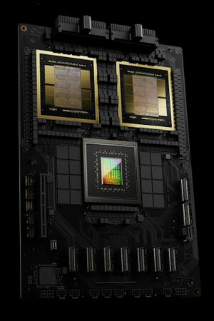
بلاكويل Blackwell هي graphics processing unit (GPU) microarchitecture developed by Nvidia as the successor to the Hopper and Ada Lovelace microarchitectures.
Named after statistician and mathematician David Blackwell, the name of the Blackwell architecture was leaked in 2022 with the B40 and B100 accelerators being confirmed in October 2023 with an official Nvidia roadmap shown during an investors presentation.[1] It was officially announced at Nvidia's GTC 2024 keynote on March 18, 2024.[2]
. . . . . . . . . . . . . . . . . . . . . . . . . . . . . . . . . . . . . . . . . . . . . . . . . . . . . . . . . . . . . . . . . . . . . . . . . . . . . . . . . . . . . . . . . . . . . . . . . . . . . . . . . . . . . . . . . . . . . . . . . . . . . . . . . . . . . . . . . . . . . . . . . . . . . . . . . . . . . . . . . . . . . . . .
التاريخ

In March 2022, Nvidia announced Hopper architecture for datacenter for AI accelerators. Demand for Hopper products was high throughout 2023's AI hype.[3] The lead time from order to delivery of H100-based servers was between 36 and 52 weeks due to shortages and high demand.[4] Nvidia reportedly sold 500,000 Hopper-based H100 accelerators in Q3 2023 alone.[4] Nvidia's AI dominance with Hopper products led to the company increasing its market capitalization to over $2 trillion, behind only Microsoft and Apple.[5]
The Blackwell architecture is named after American mathematician David Blackwell who was known for his contributions to the mathematical fields of game theory, probability theory, information theory, and statistics. These areas have influenced or are implemented in transformer-based generative AI model designs or their training algorithms. Blackwell was the first African American scholar to be inducted into the National Academy of Sciences.[6]
In Nvidia's October 2023 Investor Presentation, its datacenter roadmap was updated to include reference to its B100 and B40 accelerators and the Blackwell architecture.[7][8] Previously, the successor to Hopper was simply named on roadmaps as "Hopper-Next". Nvidia's updated roadmap emphasized the move from a two-year release cadence for datacenter products to yearly releases targeted for x86 and ARM systems.
At the Graphics Technology Conference (GTC) on March 18, 2024, Nvidia officially announced the Blackwell architecture with focus placed on its B100 and B200 datacenter accelerators and associated products, such as the eight-GPU HGX B200 board and the 72-GPU NVL72 rack-scale system.[9] Based on published power and performance figures, it appears that the B100 and B200 are the same silicon, but the former operates at 75% of the B200's clock rate.[10] Nvidia CEO Jensen Huang said that with Blackwell, "we created a processor for the generative AI era" and emphasized the overall Blackwell platform combining Blackwell accelerators with Nvidia's ARM-based Grace CPU.[11][12] Nvidia touted endorsements of Blackwell from the CEOs of Google, Meta, Microsoft, OpenAI and Oracle.[12] The keynote did not mention gaming.
Architecture
Blackwell is an architecture designed for both data-center compute applications and for gaming and workstation applications with dedicated dies for each purpose. Purported leaks indicate that the laptop dies will be code-named GN22-Xx and the corresponding GeForce RTX Mobile GPU cards will be code-named GB20x.[13] Similar to the latter notation, GB200 and GB100 are the brand names of Nvidia's Grace Blackwell data-center superchips, modules combining two Blackwell GPUs and one Arm-based Grace processor.[14]
Process node
Blackwell is fabricated on the custom 4NP node from TSMC. 4NP is an enhancement of the 4N node used for the Hopper and Ada Lovelace architectures. The Nvidia-specific 4NP process likely adds metal layers to the standard TSMC N4P technology.[15] Each of the two compute die in the data-center B100/B200 chips 104 billion transistors, a 30% increase over the 80 billion transistors in the previous generation Hopper.[16] As Blackwell cannot reap the benefits that come with a major process node advancement, it must achieve power efficiency and performance gains through underlying architectural changes.[17]
The compute die in the data-center accelerators is at the reticle limit of semiconductor fabrication.[18] The reticle limit in semiconductor fabrication is the physical size limit that lithography machines can etch a silicon die. Previously, Nvidia had nearly hit TSMC's reticle limit with GH100's 814 mm2 die. In order to not be constrained by die size, Nvidia's B100 accelerator utilizes two GB100 dies in a single package, connected with a 10 TB/s link that Nvidia calls the NV-High Bandwidth Interface (NV-HBI). NV-HBI is based on the NVLink 5.0 protocol. Nvidia CEO Jensen Huang claimed in an interview with CNBC that Nvidia had spent around $10 billion in research and development for Blackwell's NV-HBI die interconnect. Veteran semiconductor engineer Jim Keller, who had worked on AMD's K7, K12 and Zen architectures, criticized this figure and claimed that the same outcome could be achieved for $1 billion through using Ultra Ethernet rather than the proprietary NVLink system.[19] The two connected compute dies are able to act like a large monolithic piece of silicon with full cache coherency between both dies.[20] The dual die package totals 208 billion transistors.[18] Those two dies are placed on top on a silicon interposer produced using TSMC's CoWoS-L 2.5D packaging technique.[21]
Streaming multiprocessor
CUDA cores
CUDA Compute Capability 10.0 is added with Blackwell.
Tensor cores
The Blackwell architecture introduces fifth-generation Tensor Cores for AI compute and performing floating-point calculations. In the data center, Blackwell adds support for FP4 and FP6 data types.[22] The previous Hopper architecture introduced the Transformer Engine, software to facilitate quantization of higher-precision models (e.g., FP32) to lower precision, for which Hopper has greater throughput. Blackwell's second generation Transformer Engine adds support for the newer, less-precise FP4 and FP6 types. Using 4-bit data allows greater efficiency and throughput for model inference during generative AI training.[17] Nvidia claims 20 petaflops (excluding the 2x gain the company claims for sparsity) of FP4 compute for the dual-GPU GB200 superchip.[23]
See also
References
- ^ "Nvidia Corporation - Nvidia Investor Presentation October 2023". Nvidia (in الإنجليزية الأمريكية). Retrieved 2024-03-19.
- ^ "Nvidia Blackwell Platform Arrives to Power a New Era of Computing". Nvidia Newsroom (in الإنجليزية الأمريكية). Retrieved 2024-03-19.
- ^ Szewczyk, Chris (August 18, 2023). "The AI hype means Nvidia is making shiploads of cash". Tom's Hardware (in الإنجليزية الأمريكية). Retrieved March 24, 2024.
- ^ أ ب Shilov, Anton (November 28, 2023). "Nvidia sold half a million H100 AI GPUs in Q3 thanks to Meta, Facebook — lead times stretch up to 52 weeks: Report". Tom's Hardware (in الإنجليزية الأمريكية). Retrieved March 24, 2024.
- ^ King, Ian (March 19, 2024). "Nvidia Looks to Extend AI Dominance With New Blackwell Chips". Yahoo! Finance (in الإنجليزية البريطانية). Retrieved March 24, 2024.
- ^ Lee, Jane Lanhee (March 19, 2024). "Why Nvidia's New Blackwell Chip Is Key to the Next Stage of AI". Bloomberg (in الإنجليزية البريطانية). Retrieved March 24, 2024.
- ^ "Investor Presentation" (PDF). Nvidia (in الإنجليزية الأمريكية). October 2023. Retrieved March 24, 2024.
- ^ Garreffa, Anthony (October 10, 2023). "Nvidia's next-gen GB200 'Blackwell' GPU listed on its 2024 data center roadmap". TweakTown (in الإنجليزية الأمريكية). Retrieved March 24, 2024.
- ^ "NVIDIA GB200 NVL72". NVIDIA (in الإنجليزية الأمريكية). Retrieved 2024-07-04.
- ^ Byrne, Joseph (2024-03-28). "Monster Nvidia Blackwell GPU Promises 30× Speedup, but Expect 3×". XPU.pub (in الإنجليزية الأمريكية). Retrieved 2024-07-04.
- ^ Leswing, Kif (March 18, 2024). "Nvidia CEO Jensen Huang announces new AI chips: 'We need bigger GPUs'". CNBC (in الإنجليزية الأمريكية). Retrieved March 24, 2024.
- ^ أ ب Caulfield, Brian (March 18, 2024). "'We Created a Processor for the Generative AI Era,' Nvidia CEO Says". Nvidia (in الإنجليزية الأمريكية). Retrieved March 24, 2024.
- ^ WhyCry (June 8, 2024). "NVIDIA GeForce RTX 50 laptop series launch in 2025 with 16GB, 12GB and 8GB GDDR7 variants". VideoCardz. Retrieved July 4, 2024.
- ^ "NVIDIA Blackwell Platform Arrives to Power a New Era of Computing". NVIDIA Newsroom (in الإنجليزية الأمريكية). Retrieved 2024-07-04.
- ^ Byrne, Joseph (2024-03-28). "Monster Nvidia Blackwell GPU Promises 30× Speedup, but Expect 3×". XPU.pub (in الإنجليزية الأمريكية). Retrieved 2024-07-04.
- ^ Smith, Ryan (March 18, 2024). "Nvidia Blackwell Architecture and B200/B100 Accelerators Announced: Going Bigger With Smaller Data". AnandTech (in الإنجليزية الأمريكية). Retrieved March 24, 2024.
- ^ أ ب Prickett Morgan, Timothy (March 18, 2024). "With Blackwell GPUs, AI Gets Cheaper and Easier, Competing with Nvidia Gets Harder". The Next Platform (in الإنجليزية الأمريكية). Retrieved March 24, 2024.
- ^ أ ب "Nvidia Blackwell Platform Arrives to Power a New Era of Computing". Nvidia Newsroom (in الإنجليزية الأمريكية). March 18, 2024. Retrieved March 24, 2024.
- ^ Garreffa, Anthony (April 14, 2024). "Jim Keller laughs at $10B R&D cost for Nvidia Blackwell, should've used ethernet for $1B". TweakTown (in الإنجليزية الأمريكية). Retrieved April 16, 2024.
- ^ Hagedoom, Hilbert (March 18, 2024). "Nvidia B200 and GB200 AI GPUs Technical Overview: Unveiled at GTC 2024". Guru3D (in الإنجليزية الأمريكية). Retrieved April 7, 2024.
- ^ "Nvidia Blackwell "B100" to feature 2 dies and 192GB of HBM3e memory, B200 with 288GB". VideoCardz (in الإنجليزية الأمريكية). March 17, 2024. Retrieved March 24, 2024.
- ^ Edwards, Benj (March 18, 2024). "Nvidia unveils Blackwell B200, the "world's most powerful chip" designed for AI". Ars Technica (in الإنجليزية الأمريكية). Retrieved March 24, 2024.
- ^ "NVIDIA GB200 NVL72". NVIDIA (in الإنجليزية الأمريكية). Retrieved 2024-07-04.